


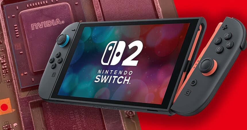
Nintendo has recently shared the technical details of its eagerly awaited Switch 2 console hybrid, generating significant buzz among gamers and tech enthusiasts alike. However, it’s crucial to recognize that what has been revealed is somewhat selective. After taking a step back from the competitive tech landscape dominated by Sony and Microsoft, there’s an eager demand for clarity and understanding of what the new console has to offer. Earlier leaks regarding the T239 processor piqued interest, but now we can delve into a more comprehensive look at its specifications and the challenges developers may encounter while adapting to this fresh system.
At the heart of the conversation about the Switch 2 is Nintendo’s assertion that it features a “custom processor built by Nvidia.” When the original Switch launched, the chipset was touted as a “custom Nvidia Tegra processor,” which turned out to be a standard Tegra X1. In contrast, the upcoming console will incorporate a system-on-chip (SoC) known as the T239, specifically designed to meet Nintendo’s specifications. While many previously leaked details have been confirmed, fresh insights offer a clearer picture.
Starting with the CPU, it’s been confirmed that Nvidia and Nintendo have opted for the ARM Cortex A78C, which utilizes the ARMv8 64-bit instruction set. Significantly, the system development kit (SDK) does not cater to 32-bit configurations. Official ARM specifications offer a variety of cache configurations, but the Switch 2 is equipped with 64K for both L1 instruction and data caches. Looking at L2, each of its eight cores gets 256K, resulting in a total of 4MB of shared L3 cache.
| Switch 2: Nvidia T239 | Switch 1: Nvidia Tegra X1 | |
|---|---|---|
| CPU Architecture | 8x ARM Cortex A78C | 4x ARM Cortex A57 |
| CPU Clocks | 998MHz (docked), 1101MHz (mobile), Max 1.7GHz | 1020 MHz (docked/mobile), Max 1.785GHz |
| CPU System Reservation | 2 cores (6 available to developers) | 1 core (3 available to developers) |
| GPU Architecture | Ampere | Maxwell |
| CUDA Cores | 1536 | 256 |
| GPU Clocks | 1007MHz (docked), 561MHz (mobile), Max 1.4GHz | 768MHz (docked), up to 460MHz (mobile), Max 921MHz |
| Memory/Interface | 128-bit/LPDDR5 | 64-bit/LPDDR4 |
| Memory Bandwidth | 102GB/s (docked), 68GB/s (mobile) | 25.6GB/s (docked), 21.3GB/s (mobile) |
| Memory System Reservation | 3GB (9GB available for games) | 0.8GB (3.2GB available for games) |
The original Switch featured the Tegra X1 with a configuration of four ARM Cortex A57 cores, setting aside one core for system tasks while providing three for developers. The Switch 2 adopts a similar framework, granting six cores for development purposes and reserving two for system use. Although the confirmed clock speeds are notable, the rationale for the mobile CPU clock running higher than in docked mode remains to be fully explained. In mobile mode, the CPU ticks at 1100MHz, while it drops to 998MHz when docked. The maximum potential of 1.7GHz may represent an unlocked capability, but whether this will actually materialize is uncertain. Historically, Nintendo has employed strategies to enhance loading times by optimizing component limits, suggesting that a faster CPU could facilitate improved asset decompression.
In the graphics arena, the Switch 2’s Ampere architecture aligns with earlier predictions, marking a departure from the original Switch’s Maxwell setup. This new architecture integrates a compact version of a consumer GPU, packed with 1536 CUDA cores, and listed clock speeds of 561MHz in handheld mode versus 1007MHz when docked. A stated maximum of 1.4GHz exists, yet it is unclear whether developers will have the ability to drive performance beyond standard parameters. Furthermore, system limitations restrict full access to the GPU’s capabilities for developers.
The Ampere GPU offers impressive performance metrics, delivering 3.072 TFLOPs in docked mode and 1.71 TFLOPs in handheld mode. Today’s gaming landscape highlights the crucial role of memory bandwidth in mobile functionality, suggesting that simple TLOPS figures can sometimes understate a GPU’s overall performance capabilities. Ultimately, the true measure of this system’s potential will hinge on the quality of the games it supports.
Additionally, both Nintendo and Nvidia confirmed that the Switch 2 will support DLSS and Ampere’s ray tracing features, with initial reports indicating the potential to achieve around 10 gigarays per second, potentially doubling to 20 in docked mode. While ray tracing can be resource-intensive, it is likely to be effectively utilized in upcoming titles, especially when the device operates in high-performance mode.
On the memory front, the earlier leaks have proved accurate: the Switch 2 will include 12GB of LPDDR5X in a dual 6GB configuration, with 102GB/s bandwidth during performance mode, dropping to 68GB/s in handheld mode. Out of the total 12GB, 3GB is allocated to the system, leaving an impressive 9GB for game development—a noteworthy upgrade from the original Switch’s 4GB, with only 3.2GB accessible for developers.
Among the standout features of the Switch 2 is a custom component known as the File Decompression Engine (FDE), designed to vastly improve storage performance compared to its predecessor. Users will appreciate 256GB of UFS storage, expandable via MicroSD Express cards up to an impressive 2TB. Notably, the efficiency of the FDE can significantly cut down loading times, as it enables file decompression to be offloaded from the CPU, hence optimizing speed and energy efficiency for this crucial task.
Regarding the display, Nintendo’s assertions hold true; the device boasts a 7.9-inch wide color gamut LCD with a crisp 1080p resolution. This display supports HDR10 and variable refresh rate (VRR) up to 120Hz. Importantly, the touchscreen retains ten-point multi-touch capability, consistent with the first Switch. However, an essential point for developers is that VRR is limited solely to the internal display, as there is currently no support for VRR through HDMI. This limitation may arise from the dock’s DisplayPort-to-HDMI converter, and many anticipate that Nintendo will seek a resolution for this issue soon.
Moreover, Game Chat emerges as a prioritized feature in the Switch 2 ecosystem, though its integration is not without challenges. This feature demands considerable system resources, compelling Nintendo to provide a Game Chat testing tool for developers to analyze potential latencies and resource strain. Monitoring the impacts of this feature on overall performance will be crucial for the gaming community.
The Nintendo SDK will fully leverage Nvidia’s DLSS, enabling performance scaling reminiscent of PC gaming. Offering options like DLSS 1x, 2x, and 3x, along with DLAA for enhanced anti-aliasing, it promises a robust gaming experience. This versatility in settings echoes trends seen in titles such as Cyberpunk 2077 and Street Fighter 6, suggesting that adaptive optimization will play a pivotal role in meeting the gaming demands of the Switch 2.
As our understanding of the Switch 2’s hardware specifications continues to take shape, it is anchored in a mix of official announcements and the leaks that have preceded. It’s evident that the hardware development has been an extensive journey, with initial groundwork laid as far back as 2021. Now that development kits are circulating among creators and an array of titles is starting to surface, we can anticipate more precise assessments of what this system will deliver. Ultimately, as always, it will be the games that determine its success, and excitement is building toward the much-anticipated unveiling on June 5th.


