


Reflect back to the excitement surrounding the rumored Switch Pro. Speculation about an upgraded version of the Switch started in 2018, but it wasn’t until 2020 that Bloomberg revealed potential features such as improved processing capabilities and stunning 4K graphics. Along with these claims, it was rumored that this Pro model would feature a dynamic seven-inch OLED display. While the original Switch eventually received an OLED upgrade, the Pro model remained largely a mystery. However, recent insights regarding the Switch 2’s processor might clarify this ongoing saga. A thorough investigation by Geekerwan and Kurnal indicates that the hardware was conceptually solidified as early as 2021. With the benefit of hindsight, it seems that the elusive Switch Pro might actually be a confluence of ideas: a fascinating combination of the Switch OLED and the foundational concepts for the upcoming console set to debut on June 5 this year.
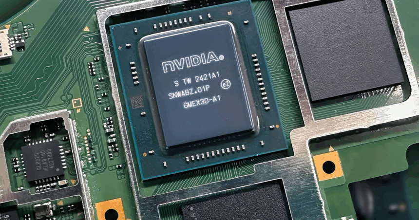
Let’s explore the recent findings shared last week on YouTube. A limited batch of Switch 2 motherboards surfaced on Chinese e-commerce platforms, prompting Geekerwan and Kurnal to acquire and analyze these components. Their focus centered on the most scrutinized feature of the Switch 2—the framework of its main processor. The Nvidia-powered T239 processor has sparked much discussion within technology communities.
Intriguingly, the architecture of Nvidia’s T239 showcases similarities with the T234, originally designed for automotive purposes. Both processors incorporate ARM A78-class CPU cores combined with a custom RTX 30-series ‘Ampere’ GPU. Constructed using Samsung’s enhanced 8nm fabrication method—an upgrade from the previous 10nm technology—this new structure has raised eyebrows in the industry. Various leaks, some originating from Nvidia, affirm that the Switch 2 will utilize an Ampere GPU associated with a modified A78 CPU cluster, all tailored for gaming tasks. Nevertheless, there have been reservations regarding the adoption of an 8nm processor, as critics argue it may be inadequate and inefficient for a portable device.
Despite this skepticism, evaluations by Geekerwan and Kurnal have dispelled many of those concerns. Their analysis suggests that the Switch 2 chip is likely built on an 8nm process, with potential incorporation of 10nm features. Impressively sized at 207mm²—larger than the Steam Deck’s 166mm²—it appears that Nintendo has engineered a more expansive Switch 2 to accommodate this considerably bigger processor. This chip is roughly 75% larger than the original Switch’s chip and twice the size of the updated processors found in the Lite and newer models. Most notably, both analyses reveal that the chip was “taped out” in 2021—essentially indicating that its design was finalized. Geekerwan compares this to Nvidia’s GA107 processor, another creation using the 8nm process that was completed in 2020 and later introduced in various GPUs (such as the RTX 3050) in 2021.
The key takeaway? Nintendo had access to the Switch 2 processor up to four years ago, which may have paved the way for an earlier launch. Given the typical timeline for processor development, whispers from Nintendo or its partners likely began surfacing around 2020 alongside the first rumors of the Switch Pro. Yet, it was in June 2021 that well-known leaker kopite7kimi revealed the processor’s name, T239, soon after its design reached the tape-out milestone.
This brings up an important question: why has the Switch 2’s release taken so long, particularly when the final silicon was ready in 2021? Industry experts in console architecture indicate that finalized silicon typically becomes available about a year ahead of a console’s launch. Since the T239 was available by 2021, the production of this chip must have been a meticulous and time-consuming process. Perhaps Nintendo initially aimed for an earlier release, yet the circumstances evolved over time. They may not have anticipated the original Switch’s sustained success, especially as sales surged during the pandemic. This led to ongoing game development for the older platform, while the manufacturing costs for the new T239 processor gradually decreased. Even if the 8nm process might feel outdated, the collaborative efforts of Nintendo and Nvidia mean that the assembly lines could still yield a new console.
The delay in launching the Switch 2 can be attributed to a lack of compelling business rationale; after all, the original console continued to perform well. Moreover, resource allocation remained focused on the existing model, as transitioning to the Switch 2 would necessitate adequate software development for the new hardware.
On a positive note, the design finalized for the Switch 2 in 2021 is not only innovative but functional. Central to its capabilities is the Nvidia Ampere GPU, which boasts not only ray tracing capabilities but also advanced machine learning functionalities. While Nintendo could have opted for a more conventional GPU structure, they harnessed the full power of Ampere’s advanced features. As a result, with the Switch 2’s specifications, it is well-positioned to attract third-party developers, echoing the successful strategy employed by the original Switch. While it may not possess raw power equivalent to some competitors, its modern GPU architecture makes it developer-friendly, complemented by a responsive and effective graphics API.
Another noteworthy aspect from the analysis videos revolves around the nature of the Ampere GPU itself. Geekerwan’s video indicates that the GPU design leans more towards the aesthetics of Nvidia’s Ada Lovelace RTX 40-series rather than the typical 30-series layout. Conversely, Kurnal cites similar designs appearing in Nvidia’s Ampere-based Jetson Nano processor. So, is it an Ada or an Ampere? Interestingly, the developer documentation for the Switch 2 specifically categorizes it as an Ampere-class GPU, without any indication of 40-series features. It is worth mentioning that most performance enhancements between Ada and Ampere stem from substantial increases in clock speeds—an RTX 3070 operates around 1.7GHz, while the 4070 peaks at approximately 2.45GHz.
Previous leaks—many of which have been substantiated—indicate that the hardware media block responsible for video encoding and decoding has shifted from Ada to T239, along with enhancements aimed at improving power efficiency. Battery life will be a vital feature of the Switch 2 that we are eager to evaluate once we get our devices at launch. Logically, the combination of an 8nm chip with all other elements of the Switch 2 operating within a mere 10W power envelope seems almost fantastical. Yet, regardless of the T239 manufacturing process, it is evident that Nintendo and Nvidia designed this chip with specific power consumption criteria in mind.
Ultimately, the discussion surrounding the design of the Switch 2 processor stems from a shared enthusiasm for wanting Nintendo’s latest hardware to excel. Still, this focus might sometimes overlook an essential truth: developers excel at maximizing potential within constraints, often yielding remarkable outcomes. Initial concerns about the Tegra X1 that powered the original Switch arose from its lackluster performance in the Nvidia Shield Android TV micro-console; nonetheless, developers managed to push the platform to incredible heights.
Though the Switch 2’s T234 might be viewed as “outdated” and its raw performance may still trail behind current-generation consoles—like the Xbox Series S—it still comes packed with impressive features and essential support from developers. Let’s not overlook the heightened expectations surrounding the upcoming release of Cyberpunk 2077, a game that has become a standard in the industry. The anticipation is palpable as we look forward to the adventures that lie ahead!


