


- Peking University transistor could outpace the best from Intel, TSMC, and Samsung
- Innovative full gate coverage enhances speed and reduces power consumption in a novel Chinese transistor design
- China may have taken a significant step forward in chip technology with this silicon-free approach
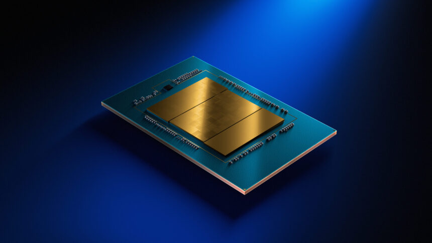
Researchers at Peking University have unveiled a potentially game-changing transistor design that could reshape the landscape of microprocessor technology.
This new silicon-free transistor utilizes a two-dimensional material known as bismuth oxyselenide.
The breakthrough is rooted in a gate-all-around (GAAFET) architecture, which allows the transistor’s gate to completely envelop the source. In contrast, the conventional FinFET designs that dominate today’s silicon-based processors only permit partial gate coverage. This full-wrap configuration significantly expands the contact area between the gate and the channel, leading to improved performance characterized by lower energy leakage and superior current regulation.
Is this the end of silicon chips as we know them?
In a study published in Nature Materials, the authors speculate that their novel 2D GAAFET could not only compete with but potentially exceed the capabilities of traditional silicon transistors in terms of both speed and energy efficiency.
The team claims their 2D transistor operates 40% faster than Intel’s latest 3nm chips while consuming 10% less power—performance metrics that place it ahead of offerings from TSMC and Samsung.
The limitations posed by partial gate coverage in existing designs lead to diminished control over current and increased energy waste. The new full-gate architecture circumvents these obstacles, providing high voltage gain coupled with extremely low power demands. They have already constructed functional small logic units using this innovative approach.
“It is the fastest, most efficient transistor ever,” boasted Peking University, with these assertions bolstered by tests performed under standardized conditions akin to those used for top commercial chips.
Professor Peng Hailin, the project lead, remarked, “If developing chips based on known materials is a ‘shortcut,’ then our introduction of 2D material-based transistors is more like ‘changing lanes.’”
Unlike the vertical designs of FinFETs, this innovative configuration resembles intricate bridges. Such a design could effectively address the miniaturization challenges plaguing silicon technology, especially as the industry strives to navigate below the 3nm mark. This could also enhance performance in ultra-compact, high-speed laptops needing advanced chips.
The research team created two novel bismuth-based materials: Bi₂O₂Se serves as the semiconductor while Bi₂SeO₅ functions as the gate dielectric.
Both materials exhibit minimal interface energy, which helps mitigate defects and reduces electron scattering.
“This permits electrons to flow almost effortlessly, akin to water streaming through a smoothly polished pipe,” Peng elaborated.
Performance assessments are substantiated by density functional theory (DFT) calculations and corroborated through rigorous physical testing on a high-precision fabrication platform at Peking University.
The researchers suggest that the transistors can be produced with existing semiconductor manufacturing techniques, simplifying the pathway for future integration.


